
Summary
120 of 122 tests pass
The campaign is complete — every planned Rev A test has been executed. The two failures are understood, dispositioned, and detailed under Issues & fixes. (RainMaker BLE provisioning and Arduino OTA were descoped for Rev A — see Plan & reference.)
Featured measurement · PWR
Power & charging deep-dive
Bench current-consumption capture of the shipped Wi‑Fi weather clock demo — a 43-minute steady-state run for the true average, plus a 10-second high-rate trace that decodes every spike, sag, and dwell — and a full USB charge cycle validating the MCP73831 charging path end to end.
Summary
What we measured
The board ran its factory firmware — fetch the local forecast over Wi‑Fi (Open‑Meteo, plain HTTP), read the on‑board SHT4x temperature/humidity sensor, and redraw the 0.96” SSD1306 OLED — while the PPK2 sourced the board and logged supply current. It was captured twice, at two rates that answer two different questions. A 43-minute run at 1 Sa/s gives the honest long-run average, because the PPK2 averages every underlying sample into each 1 s point. A 10-second run at 100 kSa/s (10 µs resolution) resolves the shape of individual events — the baseline, the periodic tick, one network exchange, and the moments the radio sleeps. A third run captured the USB charging path: a complete MCP73831 charge cycle from constant-current plateau to termination.
Every current level resolves cleanly into a known, additive load. No unexplained draw, no runaway consumption, and the transient peaks stay within the LDO/power-path budget. The headline average is the steady-state 68.9 mA; the 112 mA seen in the short trace is the active-phase draw, when sustained Wi‑Fi traffic held the radio awake. The one actionable finding is a power-optimisation opportunity, not a defect: in steady state the radio still spends roughly a third of its time awake, and dominates the average. The charge cycle additionally validates the charging path — and functionally clears the earlier suspect R5 PROG reading as an in-circuit measurement artifact.
43-min average
Wi-Fi held awake
150 µs frame
radio asleep, CPU idle
The PPK2 logs current only. Multiply by your source voltage for power — at 3.7 V the steady-state draw is ~255 mW (active phase ~415 mW). All figures below use the raw current channel.
Steady state
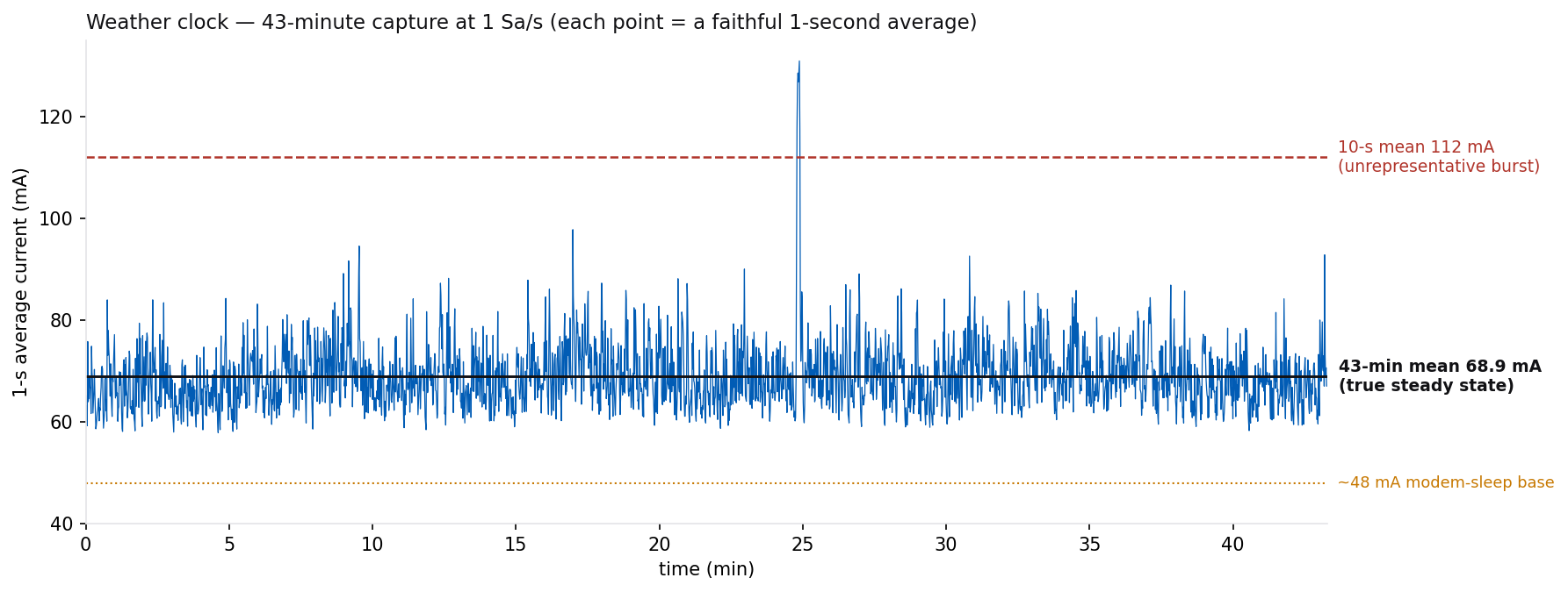
The real average: 68.9 mA over 43 minutes
A short capture can mislead. The 10-second trace below happened to land in a sustained-active phase — Wi‑Fi pinned awake at ~113 mA the whole window — and read 112 mA. Over 43 minutes the board reveals its true duty cycle: it modem-sleeps between beacons most of the time and only briefly wakes, so the long-run average settles to 68.9 mA. Each point in Fig. 1 is a faithful 1-second average (the values are smooth intermediates, not snapped to the discrete levels a subsample would show), so the lower number is real, not an artifact of the slower rate — re-binning the 100 kSa/s trace to 1 Sa/s still returns 112 mA for that window.
Two rates, two questions
Use the low rate for averages and the high rate for shapes. At 1 Sa/s the PPK2 integrates every underlying sample into each second, so a multi-minute run gives the true duty-cycled average — the number battery life should be based on. At 100 kSa/s you can dissect a single 150 µs TX frame, but a 10-second window is too short to be representative of the average.
Takeaway for the test plan: characterise average power over a window spanning many fetch cycles (tens of minutes, low rate), and reserve high-rate captures for event dissection. Figures 2 and 3 are that high-rate capture — and, as Fig. 1 shows, they sit in an unusually active stretch.
Event detail · the trace
Ten seconds, annotated
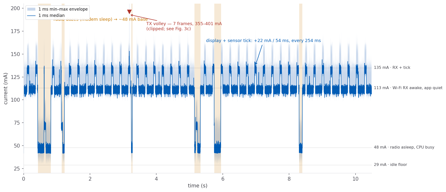
This and the next figure are the 100 kSa/s capture — the active-phase window from Fig. 1, expanded to microsecond resolution. The blue line is the 1 ms median current; the shaded band is the 1 ms min–max envelope, so sub‑millisecond transients still show as height. Amber bands mark the windows where Wi‑Fi modem sleep engaged.
Decoding the levels
The current ladder
Every feature in the trace is a stack of four independent loads. The measurement separates them cleanly — the proof is in the ticks that happened to fire while the radio was already asleep: they plateau ~25 mA lower than ticks during RX, i.e. the same render cost added to a lower base. That additivity is what lets us attribute each level below.
| Level | State | Time share |
|---|---|---|
| ~29 mA | Radio asleep, CPU idle — the true floor (brief dips only) | <1% |
| ~48–50 mA | Radio asleep, CPU active/busy-waiting | 9.5% |
| ~73 mA | Radio asleep + display tick (render on a sleeping-radio base) | — |
| ~113 mA | Wi-Fi RX awake, application quiet — the dominant dwell | 70.6% |
| ~135 mA | RX awake + display/sensor tick | 19.9% |
| 160–175 mA | Sub-ms peaks inside ticks (CPU + flash + SPI stacking) | rare |
| 355–401 mA | Wi-Fi TX frames at full RF power (7 events, all at t ≈ 3.19 s) | — |
The full story
Spike, sag, and dwell
Read chronologically, the trace tells one coherent story: a device that stays connected, ticks a display on a metronome, briefly transmits to fetch data, and grabs sleep wherever the network lets it.
The dwell at 135 mA
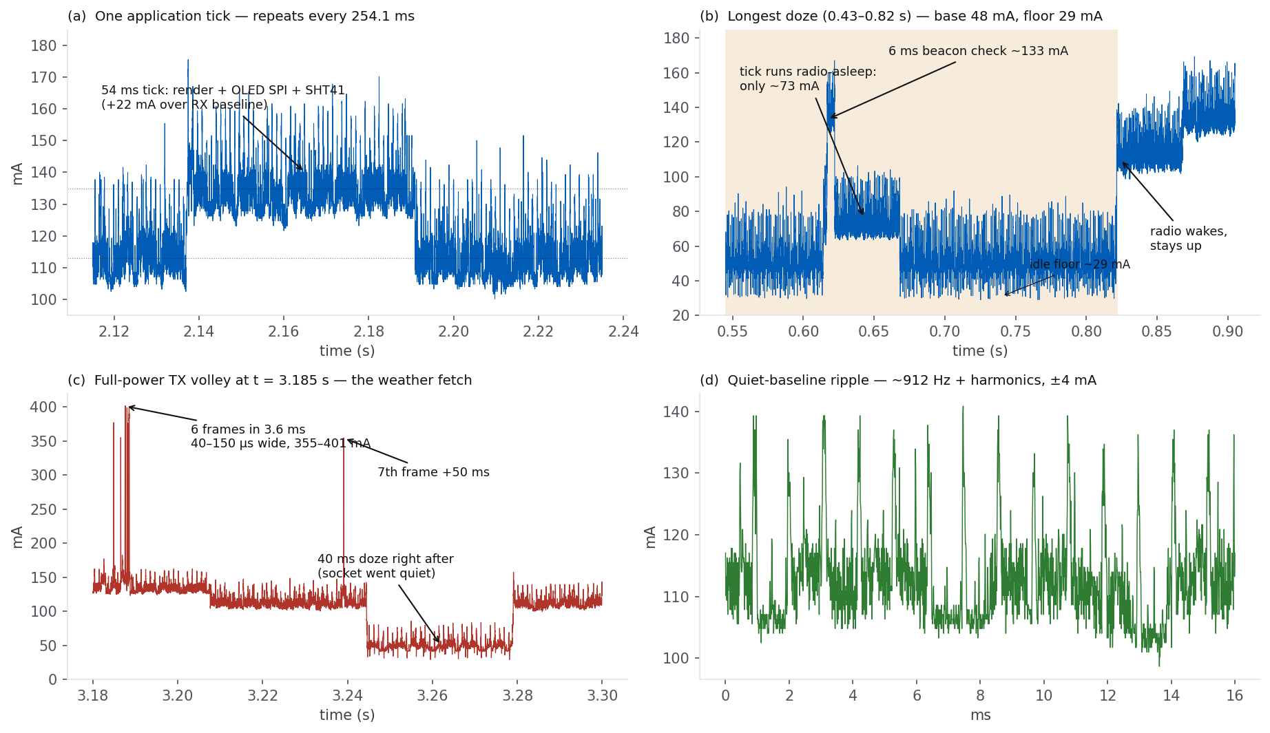
Metronomically for the entire capture — 38 ticks, period 254.1 ms, only 2.9 ms RMS jitter — the firmware wakes and does 54 ms of work: render the frame, push the buffer to the SSD1306 over SPI, poll the SHT4x. Cost: +22 mA for 54 ms on top of whatever the radio is doing.
This heartbeat is cheap: it averages only ~4.7 mA of the 112 mA active-phase total. The 254 ms period is worth a glance in firmware — it looks like delay(200) plus ~54 ms of work, so if you intended a 250 ms cadence the delay wants to be 196 ms.
The spike to 401 mA
Six Wi‑Fi transmit frames of 40–150 µs each, peaking 355–401 mA, fired within 3.6 ms — then a seventh lone frame 50 ms later, followed immediately by a 40 ms doze once the socket went quiet. This lands inside a display tick, so the application initiated it: a short request/response exchange (handshake, GET, ACKs, close) at full RF power is exactly what the weather fetch looks like from the supply rail.
The matching RX — the forecast coming back — is invisible here because it hides inside the 113 mA RX dwell. These peaks are brief enough that the entire volley moved only ~0.01 mC; they matter for the LDO/decoupling transient budget, not the energy budget.
The sags to 48 mA
Six windows (at 0.43, 1.15, 3.24, 5.15, 5.75 and 8.30 s) drop to ~48 mA as Wi‑Fi modem sleep engages — the arduino‑esp32 default WIFI_PS_MIN_MODEM working as designed. Inside the longest doze you can see 6–12 ms beacon check‑ins spaced ~102 ms apart: that is your AP’s standard 102.4 ms beacon interval, and the radio listening every 1–2 beacons.
Note the sags cluster after the 3.19 s fetch — once your own traffic stopped, the radio finally got chances to sleep. They’re rare (9.5% of the time) because ordinary LAN chatter (ARP/mDNS broadcasts) keeps yanking the radio awake. Separately, brief micro‑sags to ~29 mA show the CPU reaching true idle; between ticks it mostly sits at ~50 mA rather than the floor, hinting at busy‑waiting somewhere in the loop.
The ~912 Hz ripple
The quiet baseline carries a constant ±4 mA sawtooth at ~912 Hz plus harmonics, present in every region whether the radio is on or off. The frequency and its constancy point at the SK6812 RGB LED’s internal PWM holding a steady colour — easy to confirm by setting the LED to (0,0,0) and watching the ripple vanish. A separate ~170 Hz component appears only when the radio is awake, so that one is RF front-end housekeeping, not the display.
Event detail
The four events up close
Charging path
USB charge cycle: CC → CV → termination
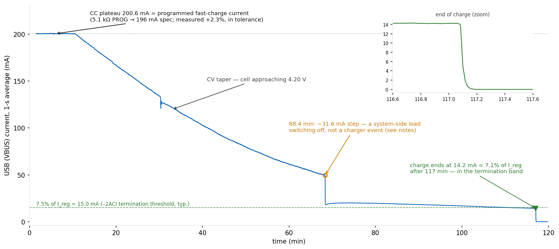
A separate run captured the battery-charging side: the PPK2 sourcing the USB VBUS rail at 1 Sa/s while the MCP73831 topped off the LiPo from a near-full state — 117 minutes from constant-current plateau through the full constant-voltage taper to end of charge, delivering 152.5 mAh at the USB side.
The charger checks out — and clears R5
- Programmed current confirms the 5.1 kΩ PROG resistor. The CC plateau sits at 200.6 mA, dead flat (±0.1 mA) — an effective RPROG of 4.99 kΩ, i.e. +2.3% against the 196 mA the BOM’s 5.1 kΩ programs, comfortably inside the resistor-plus-charger tolerance stack. The suspect in-circuit DMM reading of ~4.12 kΩ would have programmed 243 mA (−17% off — plainly absent from the data); that reading is an in-circuit artifact, the PROG pin’s internal network sitting in parallel with R5. The R5 concern is closed — the populated part behaves as a 5.1 kΩ (confirm out-of-circuit only if the site is ever reworked).
- Termination lands in the ‑2ACI band. The taper runs its full course and charging ends at 14.2 mA = 7.1% of Ireg, against the part’s 7.5%-typical termination threshold — a textbook end of charge, with the final collapse to zero shown in the inset.
- Profile shape is textbook CC/CV. ~10 min of flat CC (the cell started near full), then a smooth ~57‑min taper as the cell approaches 4.20 V, then the long shallow tail. No oscillation, no restart cycling, no thermal fold-back signature at this rate.
One open item: the 31.6 mA step at 68.4 min
Mid-taper, the USB current steps down by 31.6 mA and settles over ~5 s — then the remaining current continues the cell’s own slow taper to termination. Two fingerprints say this was not the charger: the settle is a control-loop relaxation rather than a termination edge, and the second-to-second noise after the step (±0.03 mA) is the quietest in the whole run — purely analog charging, no MCU activity. The pre-step current therefore included a ~32 mA system-side load that switched off at 68.4 min. Attribution is pending a bench note or a re-run logging VBAT and STAT alongside; it does not affect the charger conclusions above, but it should be identified before this test is marked fully closed.
Interpretation
What this means for the product
- The radio is the budget. Time spent associated and awake is what sets the average; when awake, RX alone is ~65 mA over the sleep base. Rendering, the sensor, and even the 400 mA TX peaks are rounding errors against it.
- Size the battery from 68.9 mA, not 112. At the true steady-state average a 1000 mAh cell lasts ~14.5 hours (the 112 mA active-phase number would have implied a pessimistic ~9 hours). This firmware keeps Wi‑Fi associated; it is a demo, not a low-power reference.
- The headroom is in sleep, not in the peaks. Getting the radio to sleep more — a quieter network segment, or a longer DTIM interval on the AP — drops the average further. Trimming per-tick work does almost nothing.
- Deep sleep remains the only route to multi-day life. The board’s characterised deep-sleep draw (~0.88 mA) between fetches is where a battery product would live; this always-on profile is the upper bound.
- Transient integrity looks healthy. 400 mA, 150 µs TX frames rode the rail without the baseline collapsing, so LDO output and local decoupling near the module are coping with the RF load.
- The charging path ships as designed. Fast-charge current, CV taper, and termination all land on the MCP73831‑2ACI datasheet — and the measured 200.6 mA plateau retires the R5 concern: the part behaves as the specified 5.1 kΩ, so the ~4.12 kΩ DMM reading was an in-circuit artifact, not a wrong part.
Follow-ups worth a bench session
None are blockers — they either confirm an attribution or chase the optimisation:
- Confirm the ripple source: set the SK6812 to off and re-capture the baseline. Ripple should disappear; if it doesn’t, look at the LDO or OLED charge pump.
- Chase the ~50 mA idle: find why the CPU sits at ~50 mA rather than the ~29 mA floor between ticks — likely a busy-wait or a peripheral left clocked.
- Audit the 254 ms period: confirm whether the loop delay was meant to be 250 ms, and whether the display need refresh that often at all.
- Attribute the 68.4-min load-shed: repeat the charge run logging VBAT and STAT alongside VBUS current (and keep a bench log); identify the ~32 mA system-side load that switched off mid-taper before closing the charge test.
- Quantify the sleep opportunity: re-run the 43-min capture on an isolated AP/VLAN to see how much of the steady-state awake time (~a third) is your own traffic vs. LAN broadcast chatter.
Method & provenance
How this was captured
- Instrument: Nordic Semiconductor PPK2 in source-meter mode, supplying the board and logging supply current.
- Steady-state capture: 1 Sa/s over 43.3 min (2,597 points). At this rate the PPK2 averages every underlying 100 kSa/s sample into each 1 s point, so the mean is a faithful long-run average — verified by re-binning the high-rate trace to 1 Sa/s, which reproduces its 112 mA window mean.
- Event-detail capture: 100 kSa/s (10 µs/sample) — the PPK2’s native maximum; 1,048,575 samples over 10.486 s. This window sits in an active-phase stretch (see Fig. 1).
- Charge-cycle capture: 1 Sa/s over 117 min, PPK2 sourcing the USB VBUS rail while the MCP73831T‑2ACI/OT (U5) topped off the LiPo from a near-full state; 152.5 mAh delivered.
- DUT firmware: factory Weather Clock demo — Open-Meteo forecast over plain HTTP, SHT4x indoor sensor on the Qwiic I²C bus, SSD1306 OLED over 4-wire SPI.
- Board: ESP32-S3-WROOM-1-N8, fab rev 2026-06-28.
- Analysis: levels attributed by cross-referencing envelope structure against known subsystem loads; periodicities and the ~912 Hz ripple confirmed by FFT and autocorrelation; heartbeat period and jitter from burst-edge fitting.
Raw exports: ppk-20260719T182301.csv (steady state, 1 Sa/s), ppk-20260719T144636.csv (event detail, 100 kSa/s), and USB_charge_current.csv (charge cycle, 1 Sa/s) — columns: timestamp ms, current µA, digital D0–D7. Digital channels were idle for all runs. Figures generated from the raw current channel; no smoothing beyond the stated 1 ms median used for the Fig. 2 overview line only.
Results
Every test, by subsystem
Click any row for the expected outcome, limits, measurement, and notes from the tracker. Each section ends with its full procedure from the DVT plan document.
VIS PRE PWR CHG BAT MCU GPIO I2C OLED RGB ADC BTN LED RFW RFB SYS
VIS · Visual & mechanical inspection
VIS-001Overall solder quality: tombstones, missing parts, obvious bridgespassPass
Expected: None
Measured: pass
Tracker VIS-001 · Plan §VIS-01
VIS-002D2, D3 polarity: cathode band toward V_SYS sidepassPass
Expected: Bands correct on both
Measured: pass
Tracker VIS-002 · Plan §VIS-02
VIS-003Pin-1 orientation vs silk: U1, U5, U6, D1, Q1, Q2, Q3passPass
Expected: All correct
Measured: pass
Tracker VIS-003 · Plan §VIS-03
VIS-004ESP32 module: aligned, castellations wetted, antenna cleanpassPass
Expected: Clean
Measured: pass
Tracker VIS-004 · Plan §VIS-04
VIS-005USB-C J1: all 16 pins wetted, no bridges, anchors solderedpassPass
Expected: Clean
Measured: pass
Tracker VIS-005 · Plan §VIS-05
VIS-006FPC1: 0.5 mm pins no bridges, actuator latch intactpassPass
Expected: Clean
Measured: pass
Tracker VIS-006 · Plan §VIS-06
VIS-007J2 battery conn: seated flat; J4/J5 headers straightpassPass
Expected: Clean
Measured: pass
Tracker VIS-007 · Plan §VIS-07
VIS-008SW1/SW4 buttons click mechanicallypassPass
Expected: Both click
Measured: pass
Tracker VIS-008 · Plan §VIS-08
VIS-009Board: no deep scratches, mousebite quality acceptablepassPass
Expected: OK
Measured: pass
Tracker VIS-009 · Plan §VIS-09
VIS-010Connect the OLED screen and frame, check the fitpassPass
Expected: OK
Measured: pass
Tracker VIS-010 · Plan §VIS-10
VIS-011Plug the board in breadboard, check the fitFailFail
Expected: Fail
Measured: Fail
Notes: The header spacing is a little off, which makes it hard to push the board in the breadboard.
Tracker VIS-011 · Plan §VIS-11
Full test plan for this section (from the DVT plan document)
Per board, under magnification. JLCPCB AOI catches most of this; you are double-checking the failure-prone spots.
| ID | Check | Expected | P/F |
|---|---|---|---|
| VIS-01 | Overall solder quality: tombstones, missing parts, obvious bridges | None | |
| VIS-02 | D2, D3 polarity: cathode band toward V_SYS side (D2 cathode pad at x=48.3; D3 cathode toward board interior) | Bands correct on both | |
| VIS-03 | Pin-1 orientation vs silk: U1, U5, U6, D1, Q1, Q2, Q3 | All correct | |
| VIS-04 | ESP32 module: aligned, castellations wetted, antenna area overhangs board edge cleanly — no solder, labels, or debris under/over antenna | Clean | |
| VIS-05 | USB-C J1: all 16 pins wetted, no bridges, shell anchors soldered | Clean | |
| VIS-06 | FPC1: 0.5 mm pins no bridges, actuator latch intact and opens/closes | Clean | |
| VIS-07 | J2 battery conn: seated flat, through-hole joints filled; J4/J5 headers straight | Clean | |
| VIS-08 | SW1/SW4 buttons click mechanically | Both click | |
| VIS-09 | Board: no deep scratches over traces, mousebite/edge quality acceptable for product | OK |
PRE · Unpowered electrical checks
PRE-001V_USB → GND resistance (probe D3.2)5.8k ΩPass
Expected: ≈ 9–10 kΩ, not < 1 kΩ
limits 1000 – +∞ Ω
Measured: 5.8k Ω
Tracker PRE-001 · Plan §PRE-01
PRE-002V_SYS → GND (probe D2.1)224k ΩPass
Expected: High / climbing (> 50 kΩ)
limits 50000 – +∞ Ω
Measured: 224k Ω
Tracker PRE-002 · Plan §PRE-02
PRE-0033V3 → GND (probe J4.2)42k ΩPass
Expected: > 5 kΩ and climbing (no short)
limits 5000 – +∞ Ω
Measured: 42k Ω
Tracker PRE-003 · Plan §PRE-03
PRE-004+5V pin (J5.12) → GND258k ΩPass
Expected: > 10 kΩ
limits 10000 – +∞ Ω
Measured: 258k Ω
Tracker PRE-004 · Plan §PRE-05
PRE-005Diode mode: red on D3.2 (V_USB), black on D2.1 (V_SYS)0.2 VPass
Expected: 0.15–0.40 V (SS34 forward)
limits 0.15 – 0.4 V
Measured: 0.2 V
Tracker PRE-005 · Plan §PRE-06
PRE-006Diode mode reversed: red on V_SYS, black on V_USBPass
Expected: OL
Tracker PRE-006 · Plan §PRE-07
PRE-007Diode mode: red on J5.12, black on V_SYS0.2 VPass
Expected: 0.15–0.45 V (F1 + D2 forward)
limits 0.15 – 0.45 V
Measured: 0.2 V
Tracker PRE-007 · Plan §PRE-08
PRE-008USB D+ ↔ D− (D1.1 ↔ D1.3)100000000 ΩPass
Expected: OL / > 1 MΩ (no short)
limits 1000000 – +∞ Ω
Measured: 100000000 Ω
Tracker PRE-008 · Plan §PRE-09
PRE-009USB VBUS ↔ D+ and VBUS ↔ D−Pass
Expected: No short
Tracker PRE-009 · Plan §PRE-10
PRE-010J2.1 ↔ J2.2 (battery pins)Pass
Expected: No short (> 100 kΩ)
limits 100000 – +∞ Ω
Tracker PRE-010 · Plan §PRE-11
PRE-011Diode mode: red on C3.2 (BATT+), black on J2.10.35 VPass
Expected: ≈ 0.4–0.7 V (Q3 body diode)
target 0.55000000000000004 · limits 0.3 – 0.7 V
Measured: 0.35 V
Tracker PRE-011 · Plan §PRE-12
PRE-012EN → GND / IO0 → GNDPass
Expected: No short
Tracker PRE-012 · Plan §PRE-13
Full test plan for this section (from the DVT plan document)
No power, no battery, no OLED attached. In resistance mode, capacitor charging makes readings climb — note the settled trend, not the first flash.
| ID | Measurement | Expected | Measured | P/F |
|---|---|---|---|---|
| PRE-01 | V_USB → GND resistance (probe D3.2) | ≈ 9–10 kΩ (R7 ∥ R15+R16), not < 1 kΩ | ||
| PRE-02 | V_SYS → GND (probe D2.1) | High / climbing (> 50 kΩ settled) | ||
| PRE-03 | 3V3 → GND (probe J4.2) | > 5 kΩ and climbing, no short | ||
| PRE-05 | +5V pin (J5.12) → GND | > 10 kΩ (via F1+D2 into V_SYS network) | ||
| PRE-06 | Diode mode: red on D3.2 (V_USB), black on D2.1 (V_SYS) | 0.15–0.40 V (SS34 forward) | ||
| PRE-07 | Diode mode reversed: red on V_SYS, black on V_USB | OL | ||
| PRE-08 | Diode mode: red on J5.12, black on V_SYS | 0.15–0.45 V (F1 + D2 forward) | ||
| PRE-09 | USB D+ ↔ D− (D1.1 ↔ D1.3) | OL / > 1 MΩ, no short | ||
| PRE-10 | USB VBUS ↔ D+ and VBUS ↔ D− | No short | ||
| PRE-11 | J2.1 ↔ J2.2 (battery pins) | No short (> 100 kΩ) | ||
| PRE-12 | Diode mode: red on C3.2 (BATT+), black on J2.1 | ≈ 0.4–0.7 V (Q3 body diode) | ||
| PRE-13 | EN → GND, IO0 → GND | No short |
PWR · Power-up & power rails
PWR-001Smoke test: Supply current after 5 s (5V 100mA limit)20 mAPass
Expected: 30–90 mA, stable
limits 15 – 90 mA
Measured: 20 mA
Tracker PWR-001 · Plan §PWR-01
PWR-002Smoke test: Current limit NOT hitPass
Expected: No CC indication
Tracker PWR-002 · Plan §PWR-01
PWR-003Smoke test: Components temperature after 60sPass
Expected: < warm
Tracker PWR-003 · Plan §PWR-01
PWR-004Smoke test: Green LED2Pass
Expected: ON
Tracker PWR-004 · Plan §PWR-01
PWR-005Rail voltages: V_SYS (D2.1)4.7 VPass
Expected: 4.5–4.8 V
limits 4.5 – 4.8 V
Measured: 4.7 V
Tracker PWR-005 · Plan §PWR-02
PWR-006Rail voltages: 3V3 (J4.2)3.29 VPass
Expected: 3.25–3.35 V
target 3.3 · limits 3.25 – 3.35 V
Measured: 3.29 V
Tracker PWR-006 · Plan §PWR-02
PWR-007Rail voltages: EN (U2.3)3.28 VPass
Expected: ≈ 3V3
target 3.3 · limits 3.25 – 3.35 V
Measured: 3.28 V
Tracker PWR-007 · Plan §PWR-02
PWR-008Rail voltages: BATT+ (C3.2) without batteryPass
Expected: ~0 V or drifting
Tracker PWR-008 · Plan §PWR-02
PWR-009USB power path: V_USB (D3.2)5.2 VPass
Expected: 4.75–5.25 V
target 5 · limits 4.75 – 5.25 V
Measured: 5.2 V
Tracker PWR-009 · Plan §PWR-03
PWR-010USB power path: V_SYS4.9000000000000004 VPass
Expected: V_USB − 0.2…0.45 V
Measured: 4.9000000000000004 V
Tracker PWR-010 · Plan §PWR-03
PWR-011USB power path: 3V33.29 VPass
Expected: 3.25–3.35 V
target 3.3 · limits 3.25 – 3.35 V
Measured: 3.29 V
Tracker PWR-011 · Plan §PWR-03
PWR-012USB power path: Input current idle20 mAPass
Expected: 30–90 mA
limits 15 – 90 mA
Measured: 20 mA
Tracker PWR-012 · Plan §PWR-03
PWR-013USB power path: VUSB_SENSE (U2.38)2.58 VPass
Expected: V_USB ÷ 2 ± 3 %
target 2.5 · limits 2.42 – 2.58 V
Measured: 2.58 V
Notes: Limits assume V_USB = 5.00 V; recompute ±3 % band if V_USB differs
Tracker PWR-013 · Plan §PWR-03
PWR-014USB-C orientation: A-to-C cable plug 1Pass
Expected: Powers on
Tracker PWR-014 · Plan §PWR-04
PWR-015USB-C orientation: A-to-C cable flippedPass
Expected: Powers on
Tracker PWR-015 · Plan §PWR-04
PWR-016USB-C orientation: C-to-C cable plug 1Pass
Expected: Powers on
Tracker PWR-016 · Plan §PWR-04
PWR-017USB-C orientation: C-to-C cable flippedPass
Expected: Powers on
Tracker PWR-017 · Plan §PWR-04
PWR-0183V3 static load: 150 mA across 3V3 and GND3.29 VPass
Expected: ≥ 3.25 V
limits 3.25 – +∞ V
Measured: 3.29 V
Tracker PWR-018 · Plan §PWR-05
PWR-0193V3 static load: 300 mA across 3V3 and GND3.29 VPass
Expected: ≥ 3.20 V
limits 3.2 – +∞ V
Measured: 3.29 V
Tracker PWR-019 · Plan §PWR-05
PWR-0203V3 dynamic droop: TX bursts (scope)50 mVppPass
Expected: < 150 mVpp; min > 3.0 V
Measured: 50 mVpp
Tracker PWR-020 · Plan §PWR-06
PWR-0213V3 dynamic droop: minimum voltage during TX burst (scope)3.27 VPass
Expected: min > 3.0 V
limits 3 – +∞ V
Measured: 3.27 V
Tracker PWR-021 · Plan §PWR-06
PWR-0223V3 dynamic droop: No brownout resets over 5 minPass
Expected: None
Tracker PWR-022 · Plan §PWR-06
PWR-023Min battery: Lowest supply voltage w/ no brownout2.8 VPass
Expected: ≤ 3.3 V
limits −∞ – 3.3 V
Measured: 2.8 V
Tracker PWR-023 · Plan §PWR-07
PWR-024Min battery: Voltage where board browns out2.4500000000000002 VPass
Expected: Record
Measured: 2.4500000000000002 V
Tracker PWR-024 · Plan §PWR-07
PWR-025Sleep current: @ 3.8 V0.88400000000000001 mAPass
Expected: ≈ 0.6–0.9 mA
limits 0.6 – 0.9 mA
Measured: 0.88400000000000001 mA
Tracker PWR-025 · Plan §PWR-08
PWR-026Sleep current: Same with LED2 lifted115 µAPass
Expected: < 120 µA
limits −∞ – 120 µA
Measured: 115 µA
Tracker PWR-026 · Plan §PWR-08
PWR-027+5V pin is input-only: Voltage at J5.120 VPass
Expected: ≈ 0 V / floating
target 0 · limits −∞ – 0.5 V
Measured: 0 V
Tracker PWR-027 · Plan §PWR-09
Full test plan for this section (from the DVT plan document)
PWR-01 · Smoke test (bench supply, current-limited)
No battery, no OLED. Bench PSU set to 5.00 V, current limit 100 mA, + to J5.12, − to J5.11 (this path is protected by F1 and D2 — the safest entry point).
| Check | Expected | Measured | P/F |
|---|---|---|---|
| Supply current after 5 s | 30–90 mA, stable (module boots, may idle in download mode on blank flash) | ||
| Current limit NOT hit | No CC indication | ||
| Nothing warm to touch after 60 s (U6, U5, module) | < warm | ||
| Green LED2 | ON |
PWR-02 · Rail voltages (still on bench 5 V input)
| Rail | Expected | Measured | P/F |
|---|---|---|---|
| V_SYS (D2.1) | 5.0 − (F1+D2 drop) ≈ 4.5–4.8 V | ||
| 3V3 (J4.2) | 3.25–3.35 V | ||
| EN (U2.3) | ≈ 3V3 | ||
| BATT+ (C3.2) | ~0 V or drifting (no battery — charger unpowered on this path, OK) |
PWR-03 · USB power path
Disconnect bench supply. Plug USB-C from a 5 V/≥1 A source through the USB power meter.
| Check | Expected | Measured | P/F |
|---|---|---|---|
| V_USB (D3.2) | 4.75–5.25 V | ||
| V_SYS | V_USB − 0.2…0.45 V | ||
| 3V3 | 3.25–3.35 V | ||
| Input current, idle (blank flash) | 30–90 mA | ||
| VUSB_SENSE (U2.38) | V_USB ÷ 2 ± 3 % |
PWR-04 · USB-C orientation / cable matrix
Validates CC pull-downs R3/R4 (5.1 k). Board must power in all four cases:
| Case | Powers? |
|---|---|
| A-to-C cable, plug orientation 1 | |
| A-to-C cable, plug flipped | |
| C-to-C cable, orientation 1 | |
| C-to-C cable, flipped |
C-to-C failing in both orientations while A-to-C works would indicate a CC resistor fault.
PWR-05 · 3V3 static load regulation
USB powered. Apply load across 3V3 (J4.2) and GND (J4.1): 22 Ω/2 W resistor ≈ 150 mA, then 11 Ω/2 W ≈ 300 mA.
| Load | 3V3 expected | Measured | U6 temp after 2 min | P/F |
|---|---|---|---|---|
| 150 mA | ≥ 3.25 V | |||
| 300 mA | ≥ 3.20 V | |||
| 500 mA (optional, brief) | ≥ 3.15 V |
Note: from USB, U6 drops ≈1.4 V. At 300 mA that is ~0.42 W in a SOT-25 — expect it hot (can exceed 60–80 °C). Sustained >300 mA average from USB is a thermal watch item; from battery (drop ≈0.4 V) it is a non-issue. Record temps; decide if a product-doc note is needed.
PWR-06 · 3V3 dynamic droop during WiFi TX (scope)
Flash any WiFi sketch that transmits continuously (ping flood). Scope on 3V3 at C12, AC-coupled.
| Check | Expected | Measured | P/F |
|---|---|---|---|
| Droop during TX bursts | < 150 mVpp; absolute min > 3.0 V | ||
| No brownout resets in serial log over 5 min | None |
PWR-07 · Minimum battery voltage / brownout sweep
Bench PSU as battery on J2 (correct polarity!), current limit 800 mA, USB disconnected. Run the WiFi TX sketch. Step supply 4.2 → 3.0 V in 0.1 V steps, 30 s each.
| Check | Expected | Measured | P/F |
|---|---|---|---|
| Lowest supply voltage with no reset/brownout | ≤ 3.3 V (target: WiFi stable at 3.3 V) | ||
| Voltage where board browns out | record |
This defines the usable battery range → firmware low-battery cutoff should sit ~0.1–0.2 V above the measured brownout point.
PWR-08 · Quiescent / deep-sleep current (battery)
Flash a deep-sleep sketch (sleep 60 s). Battery or bench-as-battery on J2, µA meter in series in the + lead. Wait for sleep entry.
| Check | Expected | Measured | P/F |
|---|---|---|---|
| Sleep current @ 3.8 V | ≈ 0.6–0.8 mA — dominated by green LED2 (~0.6 mA); remainder: AP2112 Iq ~55 µA + R10/R11 divider ~19 µA + DW01A ~3 µA + ESP ~10 µA + SS34 reverse leakage | ||
| (optional) Same with LED2 lifted | < 120 µA |
If sub-100 µA standby ever becomes a product goal, LED2 and the always-connected sense divider are the items to revisit — record the baseline now.
PWR-09 · +5V pin is input-only
USB powered, nothing on J5.12.
| Check | Expected | Measured | P/F |
|---|---|---|---|
| Voltage at J5.12 | ≈ 0 V / floating (D2 blocks reverse; small leakage OK) |
Document in the product manual: pin 12 is a 5 V input (fused 0.5 A), not a 5 V output.
CHG · Battery charger
CHG-001Fast-charge current into battery198 mAPass
Expected: 170–250 mA
target 196 · limits 170 – 240 mA
Measured: 198 mA
Tracker CHG-001 · Plan §CHG-01
CHG-002PROG pin (U5.5) voltage during fast charge0.998 VPass
Expected: ≈ 1.0 V
target 1 · limits 0.9 – 1.1000000000000001 V
Measured: 0.998 V
Tracker CHG-002 · Plan §CHG-02
CHG-003Yellow LED1 during chargePass
Expected: ON
Tracker CHG-003 · Plan §CHG-03
CHG-004BATT+ plateau near end of charge4.18 VPass
Expected: 4.168–4.232 V
target 4.2 · limits 4.1680000000000001 – 4.2320000000000002 V
Measured: 4.18 V
Tracker CHG-004 · Plan §CHG-04
CHG-005Termination: charge current at end15 mAPass
Expected: < 20 mA then LED1 OFF
limits −∞ – 20 mA
Measured: 15 mA
Tracker CHG-005 · Plan §CHG-05
CHG-006No battery connected (USB in)blinkPass
Expected: LED1 off or faint blink
Measured: blink
Tracker CHG-006 · Plan §CHG-06
CHG-007Charge + system running (WiFi demo): USB current442 mAPass
Expected: Record
Measured: 442 mA
Tracker CHG-007 · Plan §CHG-07
CHG-008U5 temperature during fast charge at VBAT ≈ 3.6 V44 °CPass
Expected: Record temp
Measured: 44 °C
Tracker CHG-008 · Plan §CHG-08
Full test plan for this section (from the DVT plan document)
Use a partially discharged Li-Po (3.6–3.9 V). USB powered. Measure battery current with the meter in series at J2 + lead, or as (USB input current delta).
| ID | Check | Expected | Measured | P/F |
|---|---|---|---|---|
| CHG-01 | Fast-charge current into battery | 1000 V ÷ 5.1 kΩ ≈ 196 mA, accept 170–220 mA | ||
| CHG-02 | PROG pin (U5.5) voltage during fast charge | ≈ 1.0 V | ||
| CHG-03 | Yellow LED1 during charge | ON | ||
| CHG-04 | BATT+ plateau near end of charge | 4.168–4.232 V | ||
| CHG-05 | Termination: charge current at end | < ~20 mA, then LED1 OFF | ||
| CHG-06 | No battery connected, USB in | LED1 off or faint blink (charger cycling) — record behavior; BATT+ shows ~4.2 V pulses | ||
| CHG-07 | Charge + system running (WiFi demo): total USB input current | Record; note it can exceed 500 mA → product docs should specify a ≥1 A USB source | ||
| CHG-08 | U5 temperature during fast charge at VBAT ≈ 3.6 V | Warm is normal (~0.3 W); internal thermal regulation may taper current — record temp |
BAT · Battery protection & power path
BAT-001Reverse polarity: bench supply on J2 REVERSED 4VPass
Expected: Current ≈ 0, board dead
Tracker BAT-001 · Plan §BAT-01
BAT-002Under-voltage cutoff: lower slowly to 2.3 V2.4500000000000002 VPass
Expected: DW01A cuts discharge at 2.4 ± 0.1 V
target 2.4 · limits 2.2999999999999998 – 2.5 V
Measured: 2.4500000000000002 V
Tracker BAT-002 · Plan §BAT-02
BAT-003UV recovery: raise supply back to ≈ 3.0 VPass
Expected: Board recovers and reboots
Tracker BAT-003 · Plan §BAT-02
BAT-004Switchover battery → USB: run demo on battery, plug USBPass
Expected: No reset; Q1 off, D3 takes over; V_SYS steps up to ≈ 4.6 V
Tracker BAT-004 · Plan §BAT-05
BAT-005Switchover USB → battery: unplug USB while runningPass
Expected: No reset; V_SYS drops to VBAT
Tracker BAT-005 · Plan §BAT-06
BAT-006Backfeed check: USB in, no battery — voltage at J2.14.12 VPass
Expected: Charger voltage ≈ 4.2 V region (may cycle); confirm NOT 5 V
limits −∞ – 4.4000000000000004 V
Measured: 4.12 V
Tracker BAT-006 · Plan §BAT-07
Full test plan for this section (from the DVT plan document)
Bench PSU emulates the battery for threshold tests (current limit 500 mA unless noted).
| ID | Procedure | Expected | Measured | P/F |
|---|---|---|---|---|
| BAT-01 | Reverse polarity: bench supply on J2 REVERSED, 4 V, limit 100 mA | Current ≈ 0, board dead, nothing heats; normal function after reconnecting correctly (Q3 blocks) | ||
| BAT-02 | Under-voltage cutoff: supply as battery, board running (no USB). Lower slowly to 2.3 V | DW01A cuts discharge at 2.4 ± 0.1 V → board powers off; recovers when raised to ≥ 3.0 V (may need USB blip to re-enable) | ||
| BAT-05 | Switchover, battery → USB: run demo on battery, plug USB. Watch serial log / uptime | No reset. Q1 turns off, D3 takes over; V_SYS steps up ~4.6 V | ||
| BAT-06 | Switchover, USB → battery: unplug USB while running | No reset; V_SYS drops to VBAT. Scope V_SYS (optional): dip stays > 3.0 V | ||
| BAT-07 | Backfeed check: USB in, no battery | J2.1 shows charger voltage (~4.2 V region, may cycle) — normal; confirm not 5 V |
MCU · Processor bring-up
MCU-001Plug USB to PC, blank flashFail
Expected: Enumerates as Espressif USB JTAG/serial debug unit (VID 303A, PID 1001)
Notes: Wrong part was populated at D1 (an SRV05-4 instead of the specified USBLC6-2SC6). After rework with the correct part, USB enumerates correctly. Corrected part is locked in for the next build.
Tracker MCU-001 · Plan §MCU-01
MCU-002Manual download mode: hold BOOT (SW4), tap RESET (SW1), release BOOTPass
Expected: Re-enumerates in download mode
Tracker MCU-002 · Plan §MCU-02
MCU-003Flash DVT helper firmware @ 921600 over native USBPass
Expected: Flash + verify OK
Tracker MCU-003 · Plan §MCU-04
MCU-004Serial monitor over native USB CDCPass
Expected: Boot log + helper menu visible
Tracker MCU-004 · Plan §MCU-05
MCU-005UART0 via header: 3.3 V adapter, GND→J4.1, boot log on J4.10Pass
Expected: Boot log readable; record silk orientation in Notes
Tracker MCU-005 · Plan §MCU-06
MCU-006RESET (SW1) while runningPass
Expected: Clean reset, boot log, no hang (EN RC ≈ 11 ms)
Tracker MCU-006 · Plan §MCU-07
MCU-007Timekeeping: helper mode t, 10 min vs stopwatch — drift0.16 %Pass
Expected: < 0.5 %
limits −∞ – 0.5 %
Measured: 0.16 %
Tracker MCU-007 · Plan §MCU-08
Full test plan for this section (from the DVT plan document)
| ID | Procedure | Expected | Measured | P/F |
|---|---|---|---|---|
| MCU-01 | Plug USB to PC, blank flash | Enumerates as Espressif USB JTAG/serial debug unit (VID 303A, PID 1001) — blank flash drops the ROM into download mode automatically | ||
| MCU-02 | Manual download mode: hold BOOT (SW4), tap RESET (SW1), release BOOT | Re-enumerates in download mode | ||
| MCU-03 | esptool.py flash_id / chip info | ESP32-S3, flash size 8 MB (N8), record MAC address → write on board label as S/N | ||
| MCU-04 | Flash DVT helper firmware @ 921600 over native USB | Flash + verify OK | ||
| MCU-05 | Serial monitor over native USB CDC (USB CDC On Boot: Enabled) | Boot log + sketch output visible | ||
| MCU-06 | UART0 via header: 3.3 V USB-UART adapter, GND→J4.1. Boot log expected on J4.10 ("RX" net = ESP U0TXD) at 115200; adapter TX → J4.9 | Boot log readable; note which silk label sits on which pin and record for the product manual | ||
| MCU-07 | RESET (SW1) while running | Clean reset, boot log; no hang (EN RC ≈ 11 ms from R12·C11) | ||
| MCU-08 | Timekeeping sanity: log millis() for 10 min vs wall clock | Drift < 0.5 % (crystal gross check; NTP covers accuracy in product) |
GPIO · I/O verification
GPIO-001Walking output (helper 1): LOWEST V_high across all 12 header pins3.2759999999999998 VPass
Expected: Every pin ≥ 3.1 V driven HIGH
limits 3.1 – +∞ V
Measured: 3.2759999999999998 V
Notes: Record worst pin in Notes
Tracker GPIO-001 · Plan §GPIO-01
GPIO-002Walking output: HIGHEST V_low across all 12 header pins2E-3 VPass
Expected: Every pin ≤ 0.1 V driven LOW
limits −∞ – 0.1 V
Measured: 2E-3 V
Notes: Record worst pin in Notes
Tracker GPIO-002 · Plan §GPIO-01
GPIO-003Input test (helper 2): pins reading 1 idle / 0 groundedPass
Expected: 12/12
limits 12 – 12 pins
Tracker GPIO-003 · Plan §GPIO-02
GPIO-004Auto adjacent-bridge test (helper 3): pairs passingPass
Expected: 9/9 pairs
limits 9 – 9 pairs
Tracker GPIO-004 · Plan §GPIO-03
GPIO-005IO0 idle voltage (internal pull-up only)3.2890000000000001 VPass
Expected: ≥ 3.0 V
limits 3 – +∞ V
Measured: 3.2890000000000001 V
Tracker GPIO-005 · Plan §GPIO-04
GPIO-006Cold boots to app with no buttons touched10 bootsPass
Expected: 10/10
limits 10 – 10 boots
Measured: 10 boots
Tracker GPIO-006 · Plan §GPIO-04
Full test plan for this section (from the DVT plan document)
Header GPIOs on the fabbed board: J4: IO5, IO6, IO7, IO15, IO16 · J5: IO1, IO13, IO39, IO37, IO36, IO35, IO21.
GPIO-01 · Output walking test
DVT firmware drives each pin high 1 s / low 1 s in sequence (serial announces which). Measure at the header pin, which also proves the module-pad → trace → header path.
| Pin (header) | GPIO | V_high (≥ 3.1 V) | V_low (≤ 0.1 V) | P/F |
|---|---|---|---|---|
| J4.3 | IO5 | |||
| J4.4 | IO6 | |||
| J4.5 | IO7 | |||
| J4.6 | IO15 | |||
| J4.7 | IO16 | |||
| J5.3 | IO1 | |||
| J5.4 | IO13 | |||
| J5.5 | IO39 | |||
| J5.7 | IO37 | |||
| J5.8 | IO36 | |||
| J5.9 | IO35 | |||
| J5.10 | IO21 |
GPIO-02 · Input test
Firmware enables internal pull-ups and reports pin states. Jumper each header GPIO to GND through 1 k: reported state flips 1→0; remove: returns to 1.
| Check | Expected | P/F |
|---|---|---|
| All 12 header GPIOs read 1 (pull-up), 0 when grounded | 12/12 |
GPIO-03 · Adjacent-bridge test
Firmware drives alternating pattern (odd pins high, even low, then inverted) and reads back. Catches solder bridges between neighboring header pins.
| Check | Expected | P/F |
|---|---|---|
| Read-back matches driven pattern in both phases | Match |
GPIO-04 · Strapping sanity
| Check | Expected | P/F |
|---|---|---|
| IO0 idles ≈ 3.3 V (internal pull-up only — no external resistor on this board) | ≥ 3.0 V | |
| Board cold-boots to app 10/10 times with no buttons touched (confirms floating IO3/IO45/IO46 defaults are fine) | 10/10 |
I2C · Qwiic port
I2C-001SDA idle level (J3.3)3.29 VPass
Expected: ≈ 3.3 V (R9 4.7 k pull-up)
target 3.3 · limits 3.2 – 3.4 V
Measured: 3.29 V
Tracker I2C-001 · Plan §I2C-01
I2C-002SCL idle level (J3.4)3.29 VPass
Expected: ≈ 3.3 V (R13 4.7 k pull-up)
target 3.3 · limits 3.2 – 3.4 V
Measured: 3.29 V
Tracker I2C-002 · Plan §I2C-01
I2C-0033V3 at J3.23.29 VPass
Expected: 3.25–3.35 V
target 3.3 · limits 3.25 – 3.35 V
Measured: 3.29 V
Tracker I2C-003 · Plan §I2C-02
I2C-004Bus scan with SHT4x on Qwiic cable (helper 4)Pass
Expected: Device found at 0x44
Tracker I2C-004 · Plan §I2C-03
I2C-005SHT4x temperature read26.27 °CPass
Expected: Plausible indoor temp
limits 10 – 40 °C
Measured: 26.27 °C
Tracker I2C-005 · Plan §I2C-04
I2C-006SHT4x humidity read46.6 %Pass
Expected: Plausible indoor RH
limits 10 – 90 %
Measured: 46.6 %
Tracker I2C-006 · Plan §I2C-04
I2C-007Bus at 400 kHz: scan + read (helper 4 second pass)Pass
Expected: Still OK
Tracker I2C-007 · Plan §I2C-05
I2C-008Hot-plug sensor while runningPass
Expected: Recovers on next poll, no crash
Tracker I2C-008 · Plan §I2C-06
Full test plan for this section (from the DVT plan document)
| ID | Check | Expected | Measured | P/F |
|---|---|---|---|---|
| I2C-01 | Idle levels SDA (J3.3), SCL (J3.4) | ≈ 3.3 V (R9/R13 4.7 k pull-ups) | ||
| I2C-02 | 3V3 at J3.2 | 3.25–3.35 V | ||
| I2C-03 | Bus scan with SHT4x on a Qwiic cable | Device at 0x44 found (SDA=IO8, SCL=IO18) | ||
| I2C-04 | Sensor read (existing sensorRead() code) | Plausible temp/RH (e.g., 18–30 °C indoors) | ||
| I2C-05 | Bus at 400 kHz (Wire.setClock(400000)) | Scan + read still OK | ||
| I2C-06 | Hot-plug sensor while running | Recovers on next poll, no crash |
OLED · Display subsystem
OLED-0013V3 current delta on panel attach, before initPass
Expected: +0–3 mA (pump off)
limits 0 – 3 mA
Notes: Jump of tens of mA = miswired panel — stop
Tracker OLED-001 · Plan §OLED-01
OLED-002U8g2 init (CS=10, DC=9, RST=14, SCLK=12, MOSI=11) + textPass
Expected: Renders, correct orientation
Tracker OLED-002 · Plan §OLED-02
OLED-003All-pixels-ON patternPass
Expected: Uniform, no missing rows/columns
Tracker OLED-003 · Plan §OLED-03
OLED-004Border + crosshair 1-px patternPass
Expected: Crisp lines, all edges present
Tracker OLED-004 · Plan §OLED-04
OLED-005Contrast sweep 0→255Pass
Expected: Smooth ramp, no flicker
Tracker OLED-005 · Plan §OLED-05
OLED-00610 min at SPI speed (helper 5 info screen)Pass
Expected: Stable, no artifacts
Tracker OLED-006 · Plan §OLED-09
OLED-007Cold boot straight to demo screenPass
Expected: 5/5
limits 5 – 5 boots
Tracker OLED-007 · Plan §OLED-10
Full test plan for this section (from the DVT plan document)
Power off before seating the flex. Insert fully, square, close latch. First power-up with OLED: bench/USB source with ability to observe current.
| ID | Check | Expected | Measured | P/F |
|---|---|---|---|---|
| OLED-01 | Current delta at power-on with panel attached, before init | +0–3 mA (panel idle, pump off) — a jump of tens of mA before init suggests a mis-seated/reversed flex → power off | ||
| OLED-02 | U8g2 init (SSD1306 128×64, 4W HW SPI: CS=10, DC=9, RST=14, SCLK=12, MOSI=11) + "Hello" | Text renders, correct orientation | ||
| OLED-03 | All-pixels-ON pattern | Uniform, no missing rows/columns (proves all COM/SEG through FPC) | ||
| OLED-04 | Border + crosshair 1-px pattern | Crisp single-pixel lines, edges present | ||
| OLED-05 | Contrast sweep 0→255 | Smooth brightness ramp, no flicker | ||
| OLED-09 | SPI clock at target speed (U8g2 default; SSD1306 max 10 MHz) | Stable rendering 10 min, no artifacts | ||
| OLED-10 | Cold boot straight into demo screen ×5 | Renders every time (init reliability) |
RGB · RGB status LED
RGB-001R / G / B at brightness 64 (helper 6)Pass
Expected: Correct pure colors, correct order
Tracker RGB-001 · Plan §RGB-01
RGB-002Full white (255,255,255) brieflyPass
Expected: White, no tint/flicker
Tracker RGB-002 · Plan §RGB-02
RGB-003Temperature-map colors from demo (cold→blue … hot→red)Pass
Expected: Match spec
Tracker RGB-003 · Plan §RGB-04
Full test plan for this section (from the DVT plan document)
Use core 3.x built-in neopixelWrite() / rgbLedWrite() (Adafruit_NeoPixel link issue noted previously).
| ID | Check | Expected | Measured | P/F |
|---|---|---|---|---|
| RGB-01 | Red, Green, Blue at brightness 64, 2 s each | Correct pure colors, correct order | ||
| RGB-02 | White full (255,255,255) briefly | White, no color tint/flicker (3.3 V data + 3.3 V VDD margins OK) | ||
| RGB-04 | Temperature-map colors from demo (cold→blue … hot→red) | Match spec |
ADC · Sense channels
ADC-001Bench battery 3.60 V → firmware VBAT reading (helper 7)Pass
Expected: 3.60 V ± 5 %
target 3.6 · limits 3.42 – 3.78 V
Tracker ADC-001 · Plan §ADC-01
ADC-002Repeat at 4.20 VPass
Expected: ± 5 %
target 4.2 · limits 3.99 – 4.41 V
Tracker ADC-002 · Plan §ADC-02
ADC-003Repeat at 3.20 VPass
Expected: ± 5 %
target 3.2 · limits 3.04 – 3.36 V
Tracker ADC-003 · Plan §ADC-02
ADC-004VUSB reading, USB in4.95 VPass
Expected: 4.75–5.25 V
target 5 · limits 4.75 – 5.25 V
Measured: 4.95 V
Tracker ADC-004 · Plan §ADC-04
ADC-005VUSB reading, USB out (on battery)Pass
Expected: USB-present flag works
Tracker ADC-005 · Plan §ADC-05
Full test plan for this section (from the DVT plan document)
| ID | Check | Expected | Measured | P/F |
|---|---|---|---|---|
| ADC-01 | Bench "battery" at exactly 3.60 V → firmware VBAT reading (GPIO4 × 2) | 3.60 V ± 5 % raw; record offset | ||
| ADC-02 | Repeat at 4.20 V and 3.20 V | ± 5 %; linearity note for one-point cal in production firmware | ||
| ADC-04 | VUSB reading (GPIO2 × 2): USB in | ≈ 4.75–5.25 V | ||
| ADC-05 | VUSB reading: USB out, on battery | < 0.5 V → firmware "USB present" flag works both ways |
BTN · Buttons
BTN-001SW4 BOOT: helper prints press/release, 20 ms debouncePass
Expected: 1 idle, 0 pressed, no bounce
Tracker BTN-001 · Plan §BTN-01
BTN-002SW1 RESET pressed while runningPass
Expected: Immediate clean reset
Tracker BTN-002 · Plan §BTN-02
Full test plan for this section (from the DVT plan document)
| ID | Check | Expected | P/F |
|---|---|---|---|
| BTN-01 | SW4 (BOOT/IO0): firmware prints on press/release | 1 idle, 0 pressed, no bounce issues with 20 ms debounce | |
| BTN-02 | SW1 (RESET): press while running | Immediate clean reset | |
| LED-01 | Green LED2 | On whenever 3V3 is up (any power source) | |
| LED-02 | Yellow LED1 matrix: charging / charge-done / no-battery / no-USB | ON / OFF / off-or-blink (record) / OFF |
LED · Indicator LEDs
LED-001Green LED2Pass
Expected: On whenever 3V3 is up, any power source
Tracker LED-001 · Plan §LED-01
LED-002Yellow LED1 matrix: charging / done / no-battery / no-USBPass
Expected: ON / OFF / off-or-blink (record) / OFF
Tracker LED-002 · Plan §LED-02
Full test plan for this section (from the DVT plan document)
| ID | Check | Expected | P/F |
|---|---|---|---|
| BTN-01 | SW4 (BOOT/IO0): firmware prints on press/release | 1 idle, 0 pressed, no bounce issues with 20 ms debounce | |
| BTN-02 | SW1 (RESET): press while running | Immediate clean reset | |
| LED-01 | Green LED2 | On whenever 3V3 is up (any power source) | |
| LED-02 | Yellow LED1 matrix: charging / charge-done / no-battery / no-USB | ON / OFF / off-or-blink (record) / OFF |
RFW · Wi-Fi RF
RFW-001WiFi scan (helper 8)Pass
Expected: Sees all APs the reference board sees
Tracker RFW-001 · Plan §RF-W-01
RFW-002DUT average RSSI @ 3 m, worst of 4 orientations (helper 8)-36.8 dBmPass
Expected: Record
Measured: -36.8 dBm
Notes: Four orientations: 36.8, 44.2, 33, 31 dBm
Tracker RFW-002 · Plan §RF-W-02
RFW-003Δ RSSI = |DUT − reference|, worst of 4 orientations1 dBPass
Expected: ≤ 6 dB vs reference board
limits −∞ – 6 dB
Measured: 1 dB
Notes: Δ RSSI vs reference board, worst of 4 orientations
Tracker RFW-003 · Plan §RF-W-02
RFW-004Connect to WPA2 + DHCP time (helper c)5.2 sPass
Expected: < 10 s
limits −∞ – 10 s
Measured: 5.2 s
Tracker RFW-004 · Plan §RF-W-03
RFW-005Ping ×100 from PC @ 3 m: loss0 %Pass
Expected: < 2 %
limits −∞ – 2 %
Measured: 0 %
Tracker RFW-005 · Plan §RF-W-04
RFW-006Ping ×100: average latency129 msPass
Expected: 20–200 ms (~130 ms typical over WiFi)
limits −∞ – 200 ms
Measured: 129 ms
Tracker RFW-006 · Plan §RF-W-04
RFW-007Full demo: NTP + Open-Meteo over WiFi on S3Pass
Expected: Weather + time render; note HTTPS result in Notes
Tracker RFW-007 · Plan §RF-W-07
RFW-008On battery @ 3.5 V: 5 min continuous TX (helper 9)Pass
Expected: No brownout/reset
Tracker RFW-008 · Plan §RF-W-08
Full test plan for this section (from the DVT plan document)
Run RF tests with the board on a non-metallic stand, away from your body, with the USB cable routed away from the antenna.
| ID | Procedure | Expected / Target | Measured | P/F |
|---|---|---|---|---|
| RF-W-01 | WiFi scan | Sees all APs the reference board sees | ||
| RF-W-02 | Comparative RSSI: DUT vs reference board (C6 DevKit on hand; an S3 devkit is a fairer reference if available). Same location/orientation, 3 m from AP, average ≥ 10 scans. Repeat in 4 orientations (0/90/180/270°) | Δ RSSI ≤ 6 dB vs reference in the worst orientation; record all 4 values | ||
| RF-W-03 | Connect to WPA2 AP, DHCP | Associated + IP < 10 s | ||
| RF-W-04 | ping -c 100 from PC to board at 3 m | Loss < 2 %; average latency 20–200 ms (~130 ms typical over WiFi) | ||
| RF-W-07 | Full demo (NTP + Open-Meteo fetch, plain HTTP per firmware spec) on the S3 board | Weather + time render; note whether HTTPS also works on S3 (C6 TLS hang was C6-specific — verify) | ||
| RF-W-08 | On battery at 3.5 V: 5 min continuous WiFi traffic | No brownout/reset |
RF-W-05 (throughput) and RF-W-06 (range walk) were descoped for Rev A — RF was verified by scan, comparative RSSI, association, and ping. RF-W-02 passed with a 1 dB worst-orientation delta versus the reference board.
RFB · Bluetooth LE RF
RFB-001BLE advertise (helper b), nRF Connect @ 1 m — DUT RSSI-43 dBmPass
Expected: Record
Measured: -43 dBm
Tracker RFB-001 · Plan §RF-B-01
Full test plan for this section (from the DVT plan document)
| ID | Procedure | Expected | Measured | P/F |
|---|---|---|---|---|
| RF-B-01 | BLE advertise test sketch; observe in nRF Connect at 1 m | Visible, RSSI recorded; compare vs reference board same as RF-W-02 |
RainMaker BLE provisioning (former RF-B-02/03/04) was dropped from the product — the shipping demo provisions over a WiFi captive portal, so cloud reporting and WiFi+BLE coexistence are moot. Only the BLE radio check (RF-B-01) is retained for board QA.
SYS · System-level
SYS-001Factory-fresh: erase → flash demo → cold boot full flowPass
Expected: Portal → WiFi → NTP → weather → RGB temp color → battery %
Tracker SYS-001 · Plan §SYS-01
SYS-00224 h soak on USB: unexpected rebootsPass
Expected: 0
limits −∞ – 0 count
Tracker SYS-002 · Plan §SYS-02
SYS-00324 h soak: free heap stablePass
Expected: No leak trend; record start/end heap in Notes
Tracker SYS-003 · Plan §SYS-02
SYS-004Power cycle ×20 (USB, 5 s off): successful boots20 bootsPass
Expected: 20/20
limits 20 – 20 boots
Measured: 20 boots
Tracker SYS-004 · Plan §SYS-04
SYS-005USB data hot-plug ×10 on battery: clean re-enumerations10 plugsPass
Expected: 10/10
limits 10 – 10 plugs
Measured: 10 plugs
Tracker SYS-005 · Plan §SYS-05
SYS-006Overnight charge-while-runningPass
Expected: Morning: battery full, LED1 off, still running
Tracker SYS-006 · Plan §SYS-06
SYS-007Overnight: board temperature in the morning38 °CPass
Expected: < 45 °C
limits −∞ – 45 °C
Measured: 38 °C
Tracker SYS-007 · Plan §SYS-06
SYS-008Thermal survey hottest surface (U2 / U5 / U6) — record part in Notes38 °CPass
Expected: ≤ 85 °C
limits −∞ – 85 °C
Measured: 38 °C
Tracker SYS-008 · Plan §SYS-07
SYS-009Firmware S3 pin block matches plan Appendix BPass
Expected: Match
Tracker SYS-009 · Plan §SYS-08
Full test plan for this section (from the DVT plan document)
| ID | Procedure | Expected | Measured | P/F |
|---|---|---|---|---|
| SYS-01 | Factory-fresh flow: erase flash → flash shipping demo → cold boot | Captive portal appears → configure WiFi → NTP sync → weather renders → RGB temp color → battery % shown | ||
| SYS-02 | 24 h soak on USB power, demo running, log uptime + free heap hourly | No reboot; heap stable (no leak trend) | ||
| SYS-04 | Power cycle × 20 (USB unplug/replug, 5 s off) | Boots to demo 20/20 | ||
| SYS-05 | USB data hot-plug × 10 while running on battery | No crash; CDC re-enumerates each time | ||
| SYS-06 | Overnight: battery connected, USB in, demo running | Morning: battery full, LED1 off, board < 45 °C, still running | ||
| SYS-07 | Thermal survey at steady state (WiFi demo, charging): spot-check U2 module, U5, U6 | Record temps; nothing > 85 °C surface | ||
| SYS-08 | Firmware pin-map migration check: confirm the sketch's S3 #else pin block matches Appendix B exactly (SDA 8, SCL 18, DC 9, CS 10, MOSI 11, SCLK 12, RST 14, RGB 48, VBAT 4, VUSB 2) | Match |
20. Results Summary & Sign-Off
Executed rollup for the first-article boards (individual measurements, as logged in the companion tracker). Overall: 122 measurements, 120 pass, 2 fail (98.4 %).
| Subsystem | Measurements | Pass | Fail | N/A |
|---|---|---|---|---|
| VIS visual | 11 | 10 | 1 | 0 |
| PRE unpowered | 12 | 12 | 0 | 0 |
| PWR power rails | 27 | 27 | 0 | 0 |
| CHG charger | 8 | 8 | 0 | 0 |
| BAT protection/path | 6 | 6 | 0 | 0 |
| MCU bring-up | 7 | 6 | 1 | 0 |
| GPIO | 6 | 6 | 0 | 0 |
| I2C | 8 | 8 | 0 | 0 |
| OLED | 7 | 7 | 0 | 0 |
| RGB | 3 | 3 | 0 | 0 |
| ADC | 5 | 5 | 0 | 0 |
| BTN | 2 | 2 | 0 | 0 |
| LED | 2 | 2 | 0 | 0 |
| RF WiFi | 8 | 8 | 0 | 0 |
| RF BLE | 1 | 1 | 0 | 0 |
| SYS | 9 | 9 | 0 | 0 |
| Total | 122 | 120 | 2 | 0 |
Issue log
| # | Test ID | Description | Severity | Disposition |
|---|---|---|---|---|
| 1 | MCU-001 | D1 populated with SRV05-4 instead of USBLC6-2SC6; USB data pair open, board would not enumerate | Major | Board #1 reworked (bridged D+/D−); correct part specified for next batch; JLCPCB quality claim filed; verify IC marking on first articles |
| 2 | VIS-011 | Breadboard header pitch slightly wide; hard to seat across a standard breadboard | Minor | Pull the two header rows to true 2.54 mm centers next PCB revision |
| 3 | VIS-007 | J2 battery connector footprint is not the intended part | Minor | Correct the J2 connector part/footprint in the EasyEDA library and BOM before the next build |
| 4 | VIS-003 | GPIO headers (J4/J5) have no pin labels on the top silkscreen | Minor | Add J4/J5 pin-name silkscreen next revision |
Board disposition: ☑ PASS with deviations — release candidate (two defects: D1 substitution reworked and slated for correct part next batch; header pitch, silkscreen, and battery-connector fixes rolled into the next PCB revision).
Signature: ____________________ Date: ____________
Issues & fixes
What we found, and what happens next
Rev A is a first-article validation build. These are the findings from the campaign — each with its disposition. Fixes marked “next revision” are locked into the Rev B layout.
USB data path: wrong part at D1
ResolvedMCU-001
The first-article boards arrived with an SRV05-4 populated at D1 instead of the specified USBLC6-2SC6 ESD protector, which broke USB enumeration. Board #1 was reworked with the correct part and USB enumerates and flashes normally. The corrected part is locked in for the next build, and magnified IC-marking inspection of first articles is now a standing check (VIS-03).
R5 charge-programming resistor — cleared
ResolvedCHG
An in-circuit DMM reading of ~4.12 kΩ put the 5.1 kΩ PROG resistor under suspicion. The measured charge plateau of 200.6 mA corresponds to an effective 4.99 kΩ (+2.3% of nominal), proving the populated part behaves as a 5.1 kΩ; the odd reading was an in-circuit artifact of the PROG pin’s internal network. No action needed.
Header spacing makes breadboard fit tight
Next revisionVIS-011
The row-to-row header spacing is slightly off, so pressing the board into a breadboard takes more force than it should. Header footprint spacing is corrected in the next-revision layout.
GPIO headers missing top-side labels
Next revisionVIS-003
Pin labels are printed on the back only; the next revision adds top-side silkscreen so pins can be identified while the board is seated in a breadboard.
Battery connector part change
Next revisionVIS-007
The populated battery connector is not the intended part. The correct connector is specified for the next build; polarity marking and reverse-protection behavior (BAT-01) are unaffected.
Plan & reference
The test plan’s reference data
The supporting chapters of the DVT plan: what was used, the safety rules the campaign ran under, and the as-built electrical reference for this board.
Source documents
This report is generated from these files — here are the editable originals: DVT plan (v1.2) · firmware guide · results tracker (xlsx) · DVT_Helper.ino.
Rev A scope reconciliation. RainMaker BLE provisioning (RF‑B‑02/03/04) and Arduino OTA (SYS‑03) were dropped from the product — the shipping demo provisions over a Wi‑Fi captive portal with no cloud dependency. A handful of optional first-article stress and characterization checks were also descoped (PRE‑04, BAT‑03/04/08, OLED‑06/07/08, RGB‑03, ADC‑03, RF‑W‑05/06); their IDs are left as gaps so existing references stay stable. Descoped items are omitted from the tables above.
Document & provenance
| Field | Value |
|---|---|
| Board | ESP32-S3 dev board, 76.2 × 25.4 mm, 4-layer |
| Fab data | Gerber/BOM/PnP/Flying-probe exports dated 2026-06-28 |
| Assembler | JLCPCB (LCSC parts) |
| Doc version | 1.2 — 2026-07-21 (scope reconciled with the executed tracker; supersedes v1.1 of 2026-07-03) |
Methodology & test discipline
Run sections in order. Sections VIS and PRE are unpowered and are gates: any failure there means do not apply power until resolved. First power-up (PWR-01) must be done with a current-limited supply, not a USB port on your computer.
Each test has an ID, procedure, expected result, and a blank Measured / P/F field. Fill in actual values, not just pass/fail — measured numbers are what make board #1 comparable to board #50 later. Tests marked (optional) can be skipped for later boards once the design is proven; run everything on the first articles.
Stop-on-fail rules:
-
Any rail-to-GND short in PRE → stop.
-
Current limit trips at first power-up → stop, thermal-inspect.
-
Battery tests: never connect a Li-Po until PRE-05 and BAT-01 (reverse-polarity, done with a bench supply) have passed.
References & revision notes
Source data used to build this plan: BOM_Board1_PCB1_20260628.xlsx, PickAndPlace_PCB1_2026_06_28.xlsx, FlyingProbeTesting.json (net-to-pad map), Gerber set (board outline 76.20 × 25.40 mm), Netlist_PCB1_2026-06-28.tel.
✔ Netlist verified against the as-built board (2026-07-03). The June 28 netlist was cross-checked net-by-net against the flying-probe export: all 57 shared nets match member-for-member. The four discrepancies previously found in the obsolete June 24 netlist are confirmed resolved in the current one — discard the June 24 file. For reference, the corrections now verified in both netlist and fab data:
| Item | Obsolete netlist 2026-06-24 | Netlist + fab data 2026-06-28 (verified match) |
|---|---|---|
| J5 pin 5 | IO17 | IO39 (IO17 is no-connect) |
| J4 pins 1/2, J5 pins 1/2 | 1 = 3V3, 2 = GND | 1 = GND, 2 = 3V3 |
| J4 pins 7/8 | 7 = GND, 8 = IO16 | 7 = IO16, 8 = GND |
| FPC1 pin 12 (BS2) | 3V3 | GND (correct for 4-wire SPI) |
Also confirmed in the cross-check: all no-connect pins agree (IO3/17/38/40/41/42/45/46/47, FPC1.7, FPC1.20 D2 floating, USB-C SBU pins, U1.4, U3.2 DOUT, U6.4), and net RGB_LED_DIN (U2.25 → U3.4) is simply auto-renamed NET_10 in the fab export — same connectivity. One schematic housekeeping item found: LED3 (WS2812B-V6) is an orphan symbol — present in the schematic with zero connections, absent from BOM, pick-and-place, and the board. Harmless to this build; delete it from the schematic.
Required equipment
| # | Item | Used for |
|---|---|---|
| 1 | DMM with diode mode | Everything |
| 2 | Bench PSU, 0–5 V, adjustable current limit (CC mode) | First power, battery emulation, brownout sweep |
| 3 | USB-C cables: one A-to-C, one C-to-C | USB + CC resistor validation |
| 4 | USB power meter (inline V/A) | Input current, charge current |
| 5 | 1S Li-Po with JST-XH plug (~500 mAh) — verify pigtail polarity first | Battery tests |
| 6 | µA-capable current meter (µCurrent, Joulescope, or DMM µA range) | Sleep current |
| 7 | Oscilloscope (optional but recommended) | 3V3 droop during WiFi TX, switchover transients |
| 8 | Thermal camera or IR thermometer (optional) | LDO/charger thermal |
| 9 | Qwiic SHT4x breakout + cable | I2C port test |
| 10 | VG-2864KSWEG05 OLED panel | Display tests |
| 11 | USB-UART adapter (3.3 V) | UART0 header test |
| 12 | Known-good reference board (ESP32-C6-DevKitC-1 on hand; an S3 devkit is a better RF reference if available) | Comparative RF test |
| 13 | Phone with nRF Connect (Nordic); a 2.4 GHz WiFi AP; PC with Arduino IDE (ESP32S3 Dev Module, 8 MB flash, USB CDC On Boot: Enabled) | RF + system tests |
Safety notes
-
Li-Po: JST-XH battery pigtail polarity is not standardized between vendors. Verify with the DMM that battery + lands on J2 pin 1 (the pin at board position x=68.7, y=22.4 mm, net through Q3 to BATT+) before ever plugging in. Q3 provides reverse protection, but do not rely on it.
-
Use the bench PSU in current-limit mode for every "first" — first power, first battery connect, first OLED attach.
-
Never hot-plug the OLED FPC. Power off, seat the flex fully, close the latch, then power.
-
The board has unprotected 0.5 mm-pitch FPC and USB-C pins — handle with ESD precautions.
Board reference data
4.1 Power Tree (as built)
USB-C J1 VBUS ──F?none──► V_USB ──D3 (SS34)──► V_SYS ──U6 AP2112K-3.3──► 3V3
                        │                    ▲  (EN tied to VIN)

                        ├─U5 MCP73831 ──► BATT+ ── Q3 (AO3415, rev-pol) ── J2.1 (battery +)

                        │  (PROG R5=5.1k ≈196 mA)      │

                        │                              └─ R10/R11 (100k/100k) ──► VBAT_SENSE → GPIO4

                        ├─ R15/R16 (100k/100k) ──► VUSB_SENSE → GPIO2

                        └─ Q1 gate (AO3407): USB present → Q1 OFF (battery isolated from V_SYS)

                                             USB absent (R7 10k pulls gate low) → Q1 ON, BATT+ → V_SYS
+5V header J5.12 ──F1 (0.5A polyfuse)──D2 (SS34)──► V_SYS (input only; D2 blocks output)
Battery low side: J2.2 (BATT−) ── Q2 FS8205A dual FET ── GND, controlled by U1 DW01A
LED2 (green) = 3V3 power indicator via R34 2.2k. LED1 (yellow) = charge status from U5 STAT via R6 470Ω.
D1 USBLC6-2SC6 = ESD clamp on USB D+/D− (rail pin tied to 3V3).
4.2 Expected Voltages Summary
| Net | Condition | Expected | Where to probe (side) |
|---|---|---|---|
| V_USB | USB-C 5 V source | 4.75–5.25 V | D3 anode pad, D3.2 (B) |
| V_SYS | USB powered | V_USB − 0.2…0.45 V (≈ 4.55–4.8 V) | D2/D3 cathode pad, D2.1 (B) |
| V_SYS | Battery only | V_BAT − <0.05 V (Q1 on) | same |
| 3V3 | any | 3.25–3.35 V | J4.2 / J4.12 / J5.2 (headers) |
| BATT+ | battery connected | 3.0–4.23 V | C3.2 pad (B) |
| BATT+ | charging, near full | 4.168–4.232 V (MCP73831 VREG ±0.75 %) | C3.2 |
| +5V (J5.12) | USB powered, nothing on pin | ≈ 0 V / floating (input-only pin) | J5.12 |
| VBAT_SENSE | battery connected | BATT+ ÷ 2 | U2 pin 4 (T) |
| VUSB_SENSE | USB powered | V_USB ÷ 2 (≈ 2.5 V) | U2 pin 38 (T) |
| EN | idle | ≈ 3.3 V (R12 10k pull-up) | U2 pin 3 (T) |
| IO0 | idle | ≈ 3.3 V (internal pull-up only) | U2 pin 27 (T) |
| I2C SDA/SCL | idle | ≈ 3.3 V (R9/R13 4.7k pull-ups) | J3.3 / J3.4 |
| OLED VCC | display on | 6.0–7.7 V (internal charge pump) — record | C21.2 pad (B) |
| OLED VCOMH | display on | 0.6–0.9 × VCC | C20.1 pad (B) |
4.3 Module Pin Map (ESP32-S3-WROOM-1, as built per fab data)
| Mod pin | GPIO | Net | Destination |
|---|---|---|---|
| 3 | EN | EN | SW1 reset btn, R12 10k→3V3, C11 1µ + C14 100n |
| 4 | IO4 | VBAT_SENSE | R10/R11 divider (ADC1_CH3) |
| 5/6/7 | IO5/6/7 | IO5/6/7 | J4.3 / J4.4 / J4.5 |
| 8/9 | IO15/16 | IO15/16 | J4.6 / J4.7 |
| 10 | IO17 | — | no connect |
| 11 | IO18 | I2C_SCL | J3.4 (Qwiic SCL), R13 4.7k PU |
| 12 | IO8 | I2C_SDA | J3.3 (Qwiic SDA), R9 4.7k PU |
| 13/14 | IO19/IO20 | D− / D+ | USB via D1 ESD |
| 15/16 | IO3/IO46 | — | no connect (strapping, internal defaults OK) |
| 17 | IO9 | OLED_DC | FPC1.15 |
| 18 | IO10 | OLED_DS (CS) | FPC1.13 |
| 19 | IO11 | OLED_MOSI | FPC1.19 (D1) |
| 20 | IO12 | OLED_SCLK | FPC1.18 (D0) |
| 21 | IO13 | IO13 | J5.4 |
| 22 | IO14 | OLED_RST | FPC1.14 |
| 23 | IO21 | IO21 | J5.10 |
| 24/26 | IO47/IO45 | — | no connect |
| 25 | IO48 | (RGB data) | U3 SK6812 DIN |
| 27 | IO0 | IO0 | SW4 boot btn (internal PU only) |
| 28/29/30 | IO35/36/37 | IO35/36/37 | J5.9 / J5.8 / J5.7 (free on N8 — no PSRAM) |
| 31/33/34/35 | IO38/40/41/42 | — | no connect |
| 32 | IO39 | IO39 | J5.5 (JTAG MTCK by default — fine as GPIO with USB-JTAG) |
| 36 | IO43 (U0TXD) | "RX" | J4.10 |
| 37 | IO44 (U0RXD) | "TX" | J4.9 |
| 38 | IO2 | VUSB_SENSE | R15/R16 divider (ADC1_CH1) |
| 39 | IO1 | IO1 | J5.3 (ADC1_CH0) |
⚠ Note the UART nets: the net named "TX" (J4.9) lands on the ESP32's receive pin (U0RXD/GPIO44); "RX" (J4.10) is the ESP32's transmit (U0TXD/GPIO43). This is host-perspective labeling. Verify what the silkscreen says (MCU-06) and document unambiguously in the product manual.
4.4 Connector Pinouts (as built)
J4 (bottom edge, y = 1.3 mm, left→right): 1 GND · 2 3V3 · 3 IO5 · 4 IO6 · 5 IO7 · 6 IO15 · 7 IO16 · 8 GND · 9 "TX"(→U0RXD/IO44) · 10 "RX"(→U0TXD/IO43) · 11 GND · 12 3V3
J5 (top edge, y = 24.2 mm, left→right): 1 GND · 2 3V3 · 3 IO1 · 4 IO13 · 5 IO39 · 6 GND · 7 IO37 · 8 IO36 · 9 IO35 · 10 IO21 · 11 GND · 12 +5V (input only)
J3 Qwiic (BM04B-SRSS): 1 GND · 2 3V3 · 3 SDA(IO8) · 4 SCL(IO18) — standard Qwiic order (cable: black, red, blue, yellow).
J2 battery (JST-XH 2P): 1 = BAT+ (via Q3) · 2 = BAT− (via Q2/DW01A to GND). Pin 1 is at x=68.7, y=22.4 mm.
J1 USB-C (TYPE-C-31-M-12, USB 2.0): VBUS→V_USB, CC1/CC2 each 5.1 k to GND (R4/R3), D±→D1→IO19/IO20, SBU floating, shell GND.
4.5 OLED FPC (FPC1, 30-pin 0.5 mm, VG-2864KSWEG05, §4.4.6 config)
| FPC pin | Signal | Connection |
|---|---|---|
| 1, 30 | GND guard | GND |
| 2–3 / 4–5 | C2P/C2N, C1P/C1N | C16 1µF, C17 1µF (charge pump) |
| 6 | VDDB (DC/DC in) | 3V3 |
| 7 | NC | — |
| 8 | VSS | GND |
| 9 | VDD (logic) | 3V3 |
| 10/11/12 | BS0/BS1/BS2 | GND / GND / GND (4-wire SPI) |
| 13 | CS# | IO10 |
| 14 | RES# | IO14 |
| 15 | D/C# | IO9 |
| 16/17 | R/W#, E/RD# | GND |
| 18 | D0 (SCLK) | IO12 |
| 19 | D1 (MOSI) | IO11 |
| 20 | D2 | floating (correct for serial) |
| 21–25 | D3–D7 | GND |
| 26 | IREF | R14 390 k → GND |
| 27 | VCOMH | C20 4.7 µF → GND |
| 28 | VCC (panel HV) | C21 2.2 µF → GND |
| 29 | VLSS | GND |
4.6 Probe Point Quick Reference
Best physical probe pad per key net (from flying-probe export; origin = board lower-left, top view; B = bottom side). Largest/most accessible pad chosen — header pins are through-hole and easiest.
| Net | Probe at | Side | X, Y (mm) | Notes |
|---|---|---|---|---|
| GND | J1 shell / any header GND pin | T | — | 176 pads on net |
| V_USB | D3 anode (D3.2) | B | 63.0, 10.5 | 2.0 mm pad |
| V_SYS | D2 cathode (D2.1) | B | 48.3, 23.8 | 2.0 mm pad |
| 3V3 | J4.2 header pin | T | 9.9, 1.3 | also J4.12, J5.2 |
| BATT+ | C3 + terminal (C3.2) | B | 69.5, 14.1 | 47 µF bulk cap |
| BATT− | J2.2 | T | 68.7, 19.8 | cell negative (≠ GND) |
| +5V in | J5.12 | T | 35.3, 24.2 | before F1 |
| EN | U2 pin 3 | T | 10.1, 3.7 | |
| IO0 | U2 pin 27 | T | 24.1, 21.5 | |
| VBAT_SENSE | U2 pin 4 | T | 11.4, 3.7 | |
| VUSB_SENSE | U2 pin 38 | T | 10.1, 21.5 | |
| SDA / SCL | J3.3 / J3.4 | T | 71.3, 20.5 / 19.5 | |
| USB D+ / D− (conn side) | D1.1 / D1.3 | B | 64.5, 3.4 / 1.5 | |
| Charger STAT | U5 pin 1 | B | 55.6, 21.7 | |
| Charger PROG | U5 pin 5 | B | 55.6, 24.0 | 1.0 V during charge |
| OLED VCC | C21 (pin 28 side) | B | 57.7, 16.6 | ~7 V, display on |
| OLED VCOMH | C20 (pin 27 side) | B | 56.3, 16.6 | |
| OLED IREF | FPC1.26 | B | 56.2, 14.7 | 390 k to GND |
| RGB data | U3.4 | T | 32.8, 14.4 | IO48 |
Appendix A — Known open items entering DVT
-
UART header labeling: nets "TX"/"RX" are host-perspective (J4.9 → ESP U0RXD, J4.10 → ESP U0TXD). Verify silk in MCU-06 and document.
-
Netlist rev lag — RESOLVED (2026-07-03): Netlist_PCB1_2026-06-28.tel verified to match the flying-probe data on all 57 nets, member-for-member. Remaining schematic cleanup only: delete the unconnected orphan symbol LED3 (WS2812B-V6) — it is not in the BOM, the pick-and-place, or on the board.
-
Standby current floor ≈ 0.6 mA set by green LED2 — fine for this product, but blocks any future sub-100 µA sleep claim (along with SS34 leakage and the always-on 200 k sense dividers).
-
AP2112 dissipation from USB at sustained >300 mA (PWR-05 thermal record decides if action needed).
-
USB current > 500 mA possible while charging + WiFi (CHG-07) → product docs to require ≥ 1 A supply.
Appendix B — Verified S3 pin definitions
// ESP32-S3 product board — fab rev 2026-06-28 (verified against flying-probe netlist)
define PIN_I2C_SDA 8 // Qwiic J3.3, 4.7k pull-up (R9)
define PIN_I2C_SCL 18 // Qwiic J3.4, 4.7k pull-up (R13)
define PIN_OLED_DC 9 // FPC1.15
define PIN_OLED_CS 10 // FPC1.13
define PIN_OLED_MOSI 11 // FPC1.19
define PIN_OLED_SCLK 12 // FPC1.18
define PIN_OLED_RST 14 // FPC1.14
define PIN_RGB 48 // SK6812 DIN
define PIN_BOOT_BTN 0 // SW4, internal pull-up only
define PIN_VBAT_SENSE 4 // ADC1_CH3 = BATT+ / 2 (R10/R11 100k/100k)
define PIN_VUSB_SENSE 2 // ADC1_CH1 = V_USB / 2 (R15/R16 100k/100k)
// Free header GPIOs — J4: 5, 6, 7, 15, 16 J5: 1, 13, 39, 37, 36, 35, 21
// UART0: GPIO43 (U0TXD) on J4.10, GPIO44 (U0RXD) on J4.9
// No-connect on this board: IO3, IO17, IO38, IO40, IO41, IO42, IO45, IO46, IO47
Appendix C — DVT helper firmware
One Arduino sketch, serial-menu driven over native USB CDC. Menu keys and the DVT IDs they exercise: 1 GPIO walking output (GPIO-01) · 2 GPIO input/pull-up report (GPIO-02, BTN-01) · 3 adjacent-bridge test (GPIO-03) · 4 I2C scan + SHT4x 100k/400k (I2C-01..06) · 5 OLED pattern cycle (OLED-02..05/09) · 6 RGB R/G/B/W (RGB-01/02/04) · 7 ADC dump VBAT×2 / VUSB×2 (ADC-01/02/04/05) · 8 WiFi scan + RSSI average (RF-W-01/02) · c connect + hold / ping (RF-W-03/04) · 9 continuous WiFi TX flood (PWR-06/09, RF-W-08) · h HTTP throughput (optional sanity, not a Rev A gate) · s deep-sleep 60 s (PWR-08) · b BLE advertise (RF-B-01) · t timekeeping 10 min (MCU-08) · i board info / MAC · w set WiFi credentials (NVS) · m menu. Build settings: ESP32S3 Dev Module, 8 MB flash, partition “8M with spiffs (3 MB APP / 1.5 MB SPIFFS)”, USB CDC On Boot: Enabled, PSRAM Disabled. Library: U8g2; everything else ships with arduino-esp32 core 3.x.
Engineering report for the Rev A design-verification build. Values are bench measurements on first-article hardware; production specifications may change. Board photos, guides, and downloads live on the product page.